MEMS ultrasonic mic and amplifier
1kHz to 80kHz equalising amplifier for ultrasonic microphone

intro
MEMS mic amplifier - prototype design and SMD soldering
Recently Make magazine featured an article about a bat monitor. I have a lot of those guys flying around my back yard at night, so I was intrigued to listen to them chirping around in the ultra-sonic part of the sound spectrum.
The amplifier circuit around a Knowles MEMS mic presented there looked practical, but too simple and not reaching its potential in some ways that I could just not copy when building one for myself (too many amps just not doing enough).To be clear, the circuit there was fine and serving its purpose. It was focused on an easy amlifier circuit and then goes further into the conversion and analysis of signals. I will not do that for now. So, if you are interested: link to article, german make magazine. There are also a lot of good projects out there when it comes to further analysing the signals. I will write about that in the future.
Anyways, so I will let you know how I went about the design to give a corrected frequency response adjusted to the characteristics of the microphone. Furthermore I will show you how I tackled the soldering of the SMD mic that only has unreachable pads at the bottom of the package with my new reflow soldering oven.
Keep on reading if you are interested in the following topics:
- analog amplifier circuits
- equalizers
- frequency response correction
- negative impedance converters
- custom PCBs
- SMD soldering
amplifier design
This article will focus on the amplifier interfacing an analog output MEMS microphone on one hand and an ADC that is not included in this design on the other hand. The block diagram depicts a possible system for full data acquisition and analysis.

The microphone chosen for the task at hand is a Knowles SPU0410LR5H-QB MEMS microphone. One of the main reasons for chosing this device is its detailed specification over an extended frequency range up to 80 kHz. Our ultra-sonic MEMS microphone amplifier will be designed to shine in a frequency range between 1 kHz and 80kHz. This covers the frequency of interest for bat monitoring (and potentially many other applications). If you are interested in learning more about MEMS mics I recommend this guide by Analog Devices: Analog and Digital MEMS-Microphone Design Considerations. An analog output type is discussed in this article since the digital ones are usually designed with lower frequency applications in mind.
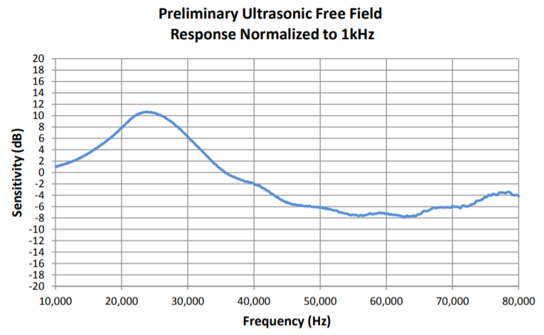
The main task of the amplifier is to provide ample gain while simultaneously correcting the uneven frequency response of the MEMS microphone. Could you live without this correction, you might ask. Well, it depends. Correcting the frequency response definitely makes this amplifier more interesting to investigate. Should that not justify doing it already? But there are more good reasons to do this. The varying sensitivity of the mic will lead you to over emphasize the 20 kHz to 30 kHz range. This will lead to clipping in that range or insufficient sensitivity in the higher frequencies. This might cause you to miss a lot of the bat talk. They use different frequencies for purposes, such as echo navigation and communication. Furthermore the frequency ranges are species dependent. To be able to successfully track everything that is going on around your bats you should employ this equalising technique.
The main task of the amplifier is to provide ample gain while simultaneously correcting the uneven frequency response of the MEMS microphone. Could you live without this correction, you might ask. Well, it depends. Correcting the frequency response definitely makes this amplifier more interesting to investigate. Should that not justify doing it already? But there are more good reasons to do this. The varying sensitivity of the mic will lead you to over emphasize the 20 kHz to 30 kHz range. This will lead to clipping in that range or insufficient sensitivity in the higher frequencies. This might cause you to miss a lot of the bat talk. They use different frequencies for purposes, such as echo navigation and communication. Furthermore the frequency ranges are species dependent. To be able to successfully track everything that is going on around your bats you should employ this equalising technique.
MEMS mic frequency response
The overall gain is set to ~450. The reasoning behind this is given in more detail on the project page. It is adequate for amplifying bat sounds that cause the microphone to produce µV-level signals to interface to a 3.3V referenced fast ADC in a µC. I will update this article in case I tune the circuit during further testing.
The gain is provided by a two stage inverting gain configuration using a dual TSV992. This op-amp is a good choice for the task. Mainly bandwidth, operating voltage range, price and availability were considered (if you need more details, let me know in the comments). The gain is set to:
The frequency range the equalizer stage is effective in is defined by the passive components, of the equalizer stage, mainly C6, and the emulated coil that is formed by the NIC (negative impedance converter, U2B, C7). In general the idea is to create a transfer function that is inverse to that of the mic displayed above.
I used the faster TSV992 (20MHz GBW) for the inverting gain stages for flexibility in the design in case a higher gain is desired and to be able to see how the if the mic still produces usabel results beyond the specified 80kHz. For a gain of 450 and the frequency rang up to 80kHz, the MCP4677 can be used in all stages. It is a pin compatible drop-in replacement.
The gain is provided by a two stage inverting gain configuration using a dual TSV992. This op-amp is a good choice for the task. Mainly bandwidth, operating voltage range, price and availability were considered (if you need more details, let me know in the comments). The gain is set to:
- gain (st1, st2) = (- 10kR / 470R)² = 453
The frequency range the equalizer stage is effective in is defined by the passive components, of the equalizer stage, mainly C6, and the emulated coil that is formed by the NIC (negative impedance converter, U2B, C7). In general the idea is to create a transfer function that is inverse to that of the mic displayed above.
I used the faster TSV992 (20MHz GBW) for the inverting gain stages for flexibility in the design in case a higher gain is desired and to be able to see how the if the mic still produces usabel results beyond the specified 80kHz. For a gain of 450 and the frequency rang up to 80kHz, the MCP4677 can be used in all stages. It is a pin compatible drop-in replacement.
equalizing amplifier schematic
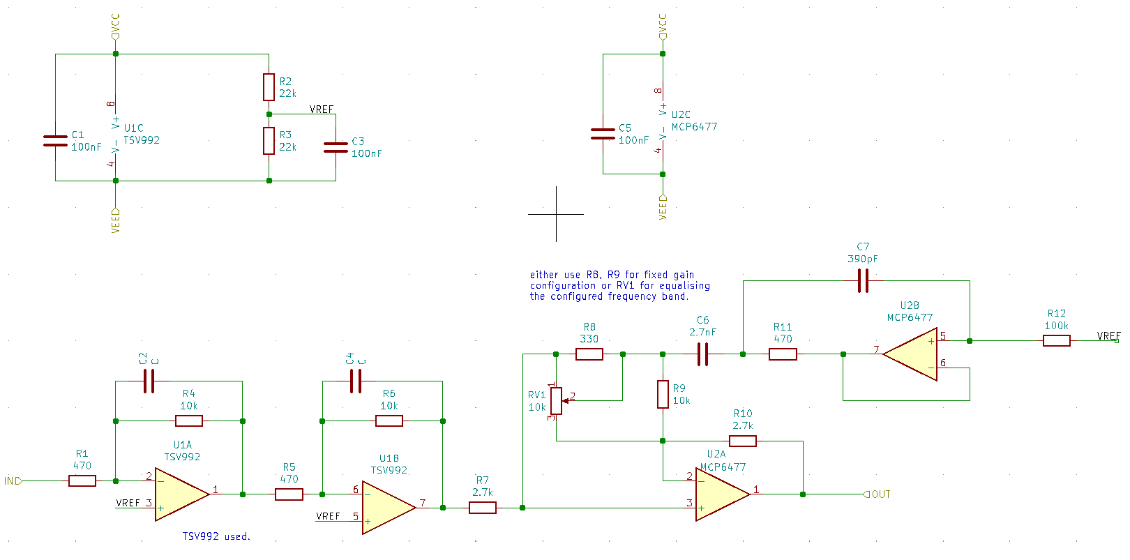
I will not give a detailed account of the NIC inductance element here, but just point you to the referenced equalizer circuit and description by TI: TI audio circuits pt.3. The equlaizer circuit and the "simulated inductor" are described there in some, but not great detail.
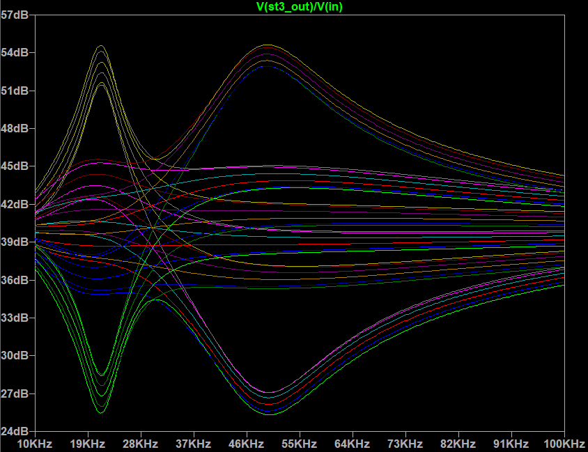
The circuit with two equalizer stages that produced the simulation output showing the flexibility in frequency responses is also described on the project page. Here I just present the result, so that we can move on to the PCB and soldering. It shows the output of stage 3, which entails the parallel equalizers referenced to the mic output. Parameters are the potentiometer settings of the equalizer stages (dimensioning of parts, see project page).
The circuit with two equalizer stages that produced the simulation output showing the flexibility in frequency responses is also described on the project page. Here I just present the result, so that we can move on to the PCB and soldering. It shows the output of stage 3, which entails the parallel equalizers referenced to the mic output. Parameters are the potentiometer settings of the equalizer stages (dimensioning of parts, see project page).
pcb prototype production
The schematic and layout were generated using KiCad 5.1.2. I used a hierarchical design even with this small circuit, so that the microphone can easily be exchanged, the connectivity on the board is isolated from the amplifier part and that it can easily be extended with more parallel equalizer bands.
board schematic

Furthermore I created a symbol and footprint for the MEMS mic which was not yet available in the main KiCad library. For the rest standard library components are used.
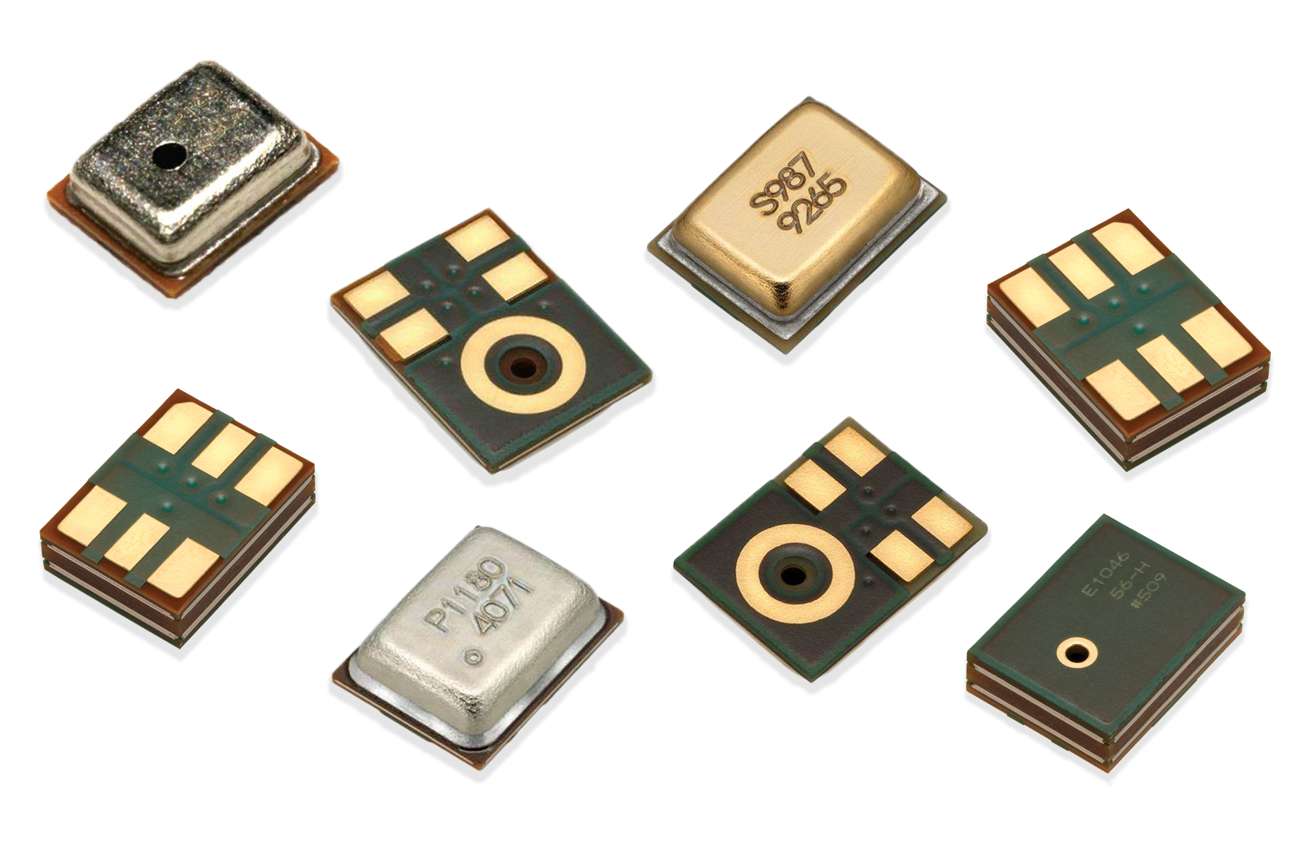
The MEMS mic is also the reason why I chose to make a PCB for this project. I already encountered the problem that some modern sensors are not available in hand solderable packages. So I finally decided to equip myself with SMD soldering capabilities at home to be more flexible in chosing components.
The MEMS mic is also the reason why I chose to make a PCB for this project. I already encountered the problem that some modern sensors are not available in hand solderable packages. So I finally decided to equip myself with SMD soldering capabilities at home to be more flexible in chosing components.
Knowles SiSonic MEMs mics. (photo taken from Knowles product page, linked above).
The rest of the layout is not overly complex and could have been done on a breadboard or using similar prototyping methods.
The two layer board has a solid GND layer on the bottom and the top flooded with the 3.3V supply. All other connections could be routed almost entirely on the top signal layer.
The two layer board has a solid GND layer on the bottom and the top flooded with the 3.3V supply. All other connections could be routed almost entirely on the top signal layer.

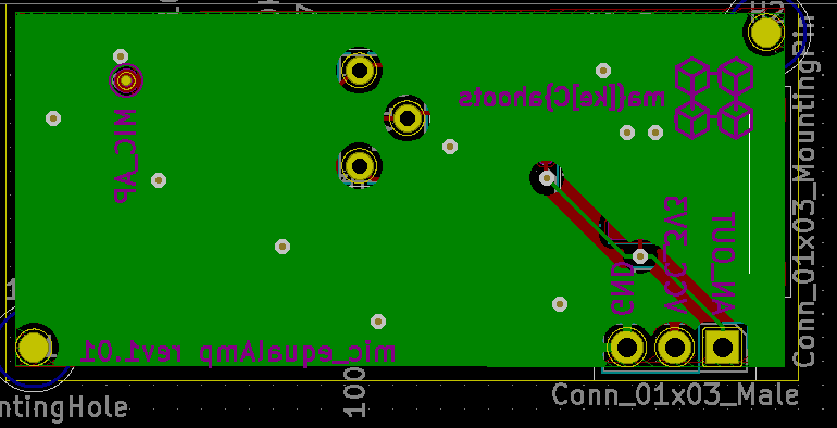
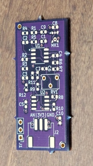
Finally the board was ordered at OSHpark.com, since I made very good experiences with them in the past. For KiCad they support submission of the project files so that you can save time for the gerber export. In the project files you additionally find gerbers if you want to use them for other purposes. I generated them to get a offer from JLCpcb. Unfortunately they did not have the parts I needed. Otherwise that can also be an option around SMD soldering at home. They offer PCB production and assembly services at low price points.
When the boards arrived, I was already thrilled to check out my new SMD reflow oven.
When the boards arrived, I was already thrilled to check out my new SMD reflow oven.
smd soldering
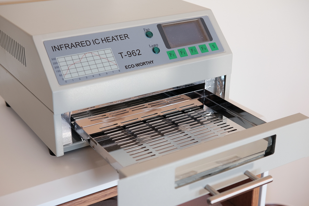
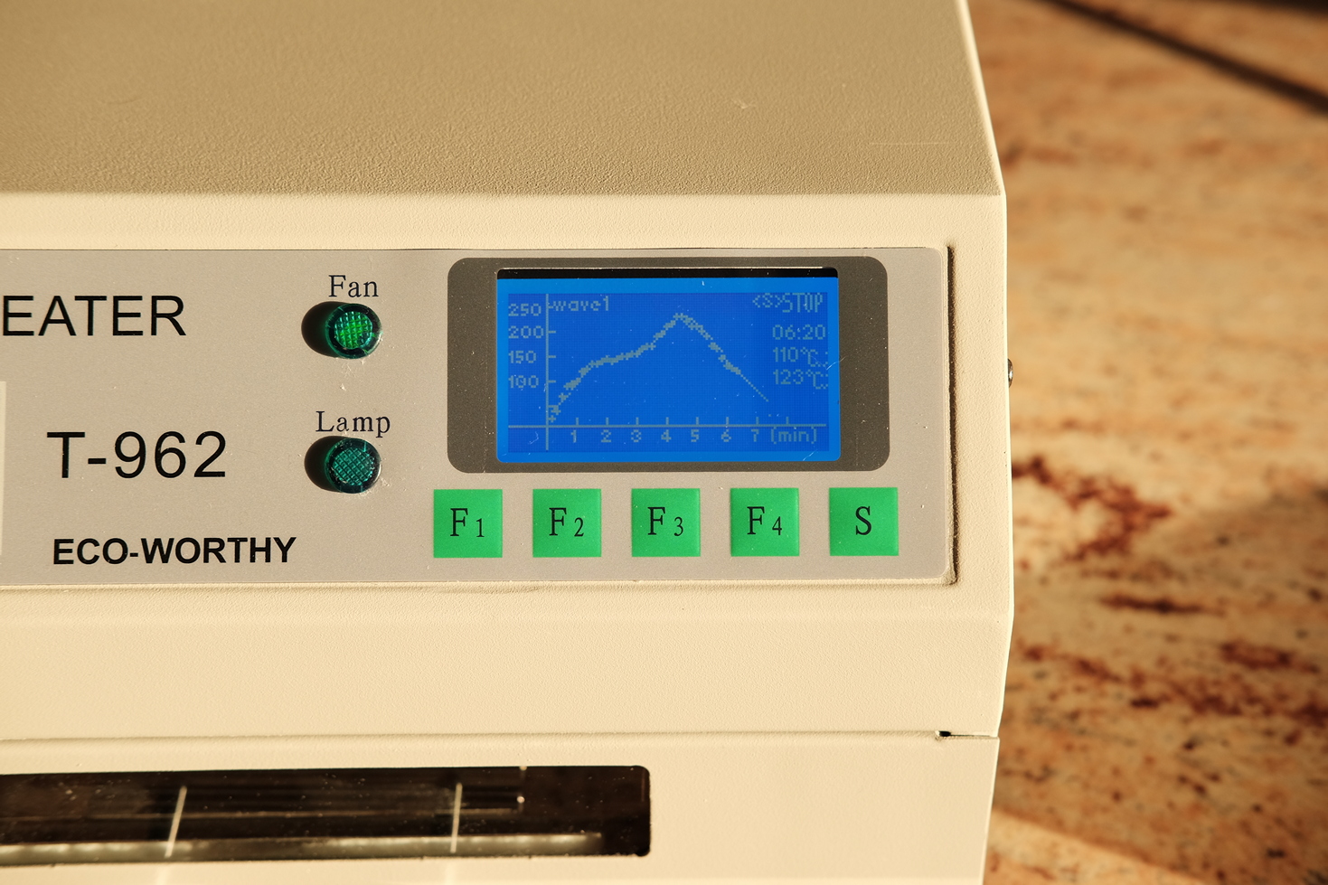
Not to be restricted to circuit boards and sensor kits available, I decided to go into SMD soldering at home. Therefore I got a Eco-Worthy T962 (available for € 169.99 in 03/2021).
So far I can only speak to the experience soldering this very small board. But the results are fantastic. The profile takes 7 minutes to complete and everything was soldered properly.
The solder paste was applied using a syringe. The product used was Chip Quik TS391AX and some additional tips SMDTA30 both available from digikey. The solder paste is temperature stable and can be stored at room temperature, as opposed to many standard pastes that need refrigaration adn still have short shelf life after being opened. So far I am also very happy with that. Will let you know in future posts about shelf life after opening and if soldering results stay positive.

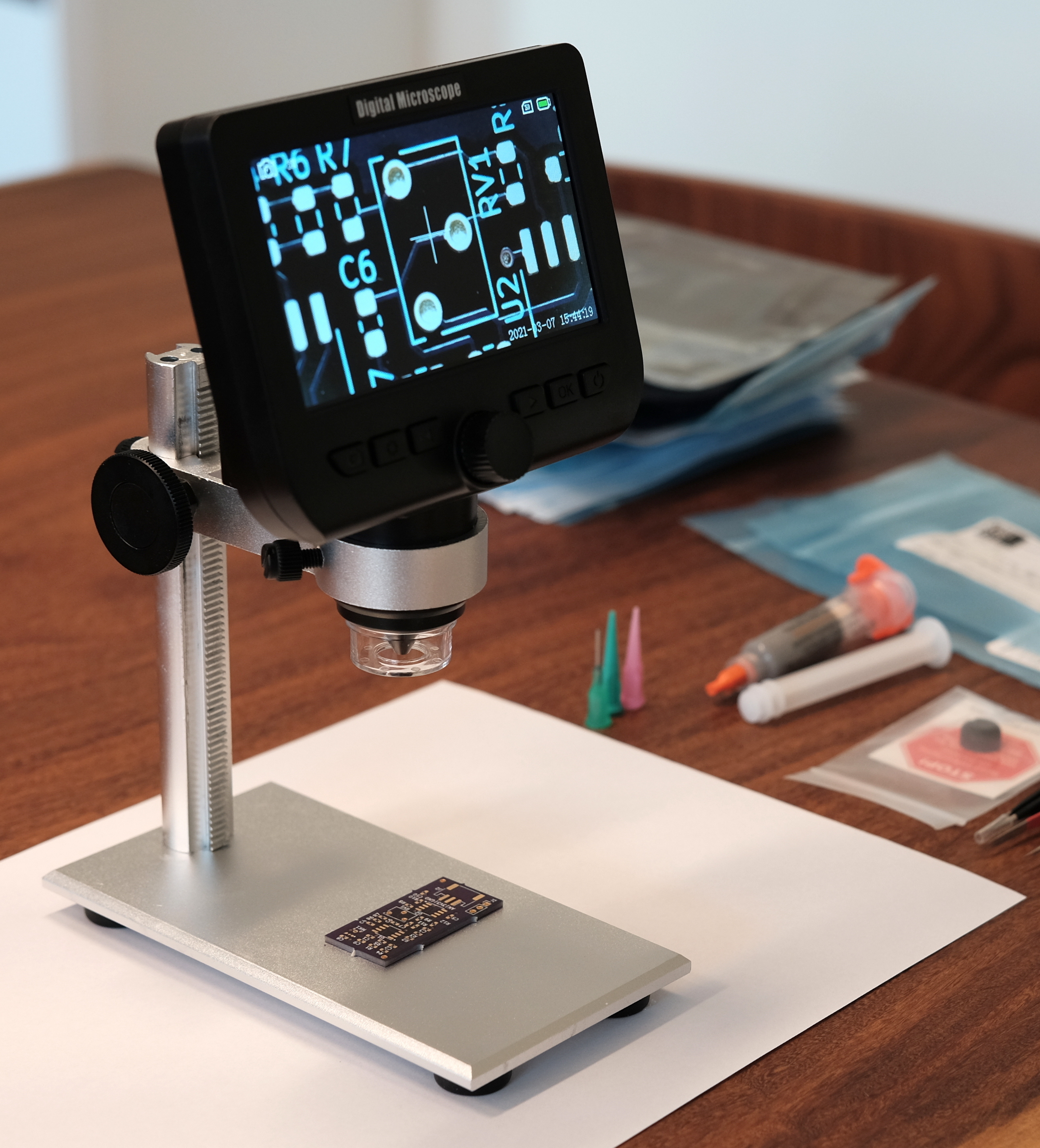
For the task of applying paste and inspecting placement as well as inspection of solder joints, I used my Yinama USB microscope that greatly helps plaacing and inspecting small SMD components. It offers 1000x magnification and can be used to store images on an SD card or directly be accessed via app from your smartphone.
I generally went for 0603 components. This size is suitable for resoldering by hand and can still easily be done without a microscope or other special equipment. The magnification helped in assessing the amount of paste applied and component placement. I also used it to inspect the results afterwards.
I generally went for 0603 components. This size is suitable for resoldering by hand and can still easily be done without a microscope or other special equipment. The magnification helped in assessing the amount of paste applied and component placement. I also used it to inspect the results afterwards.
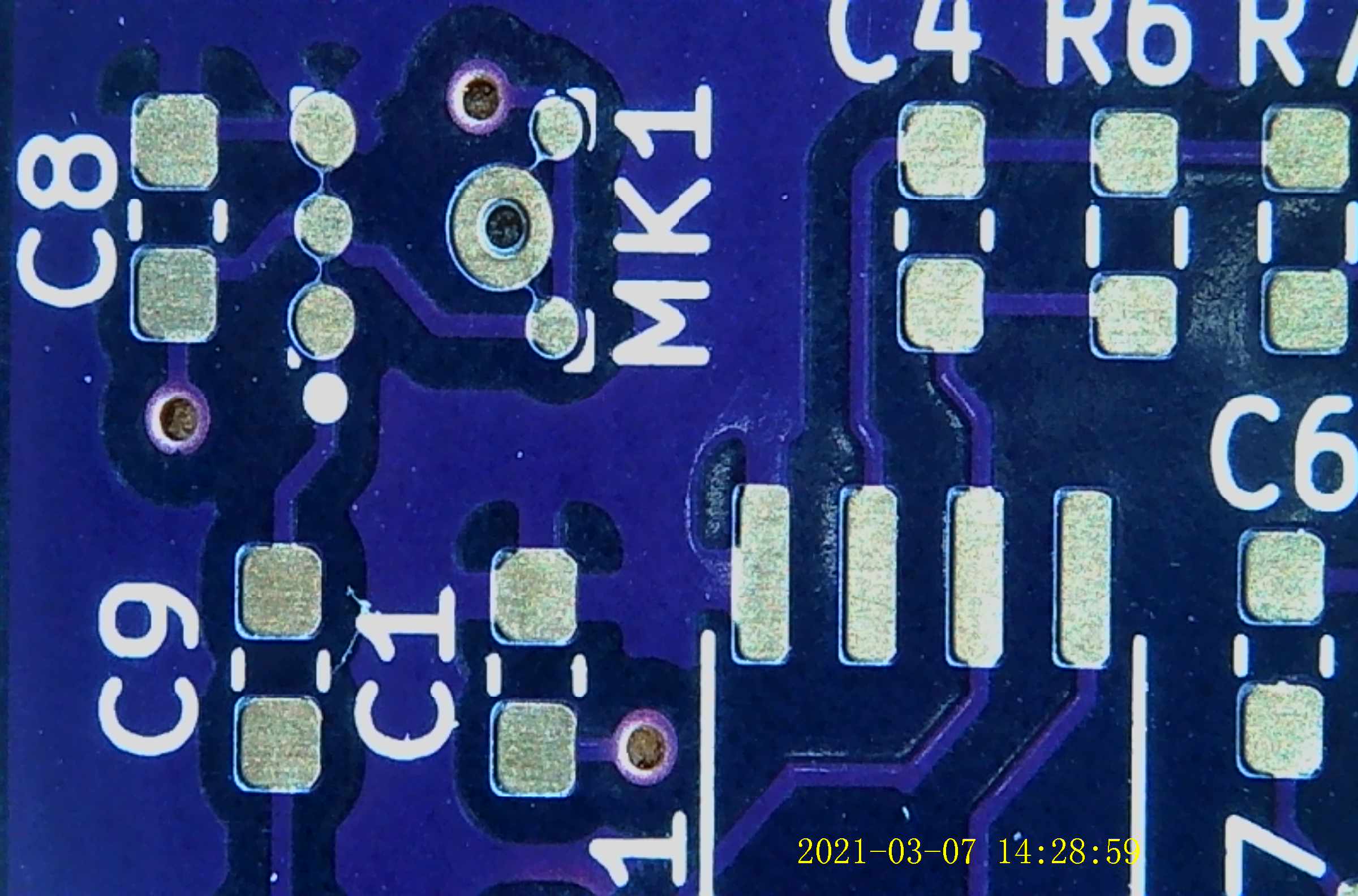

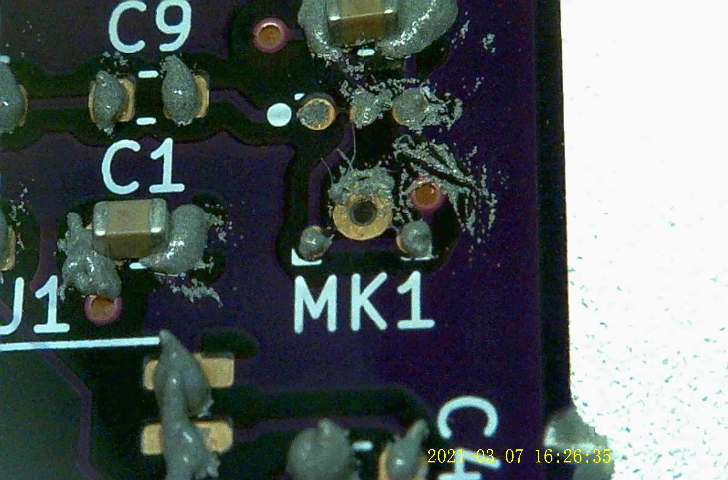
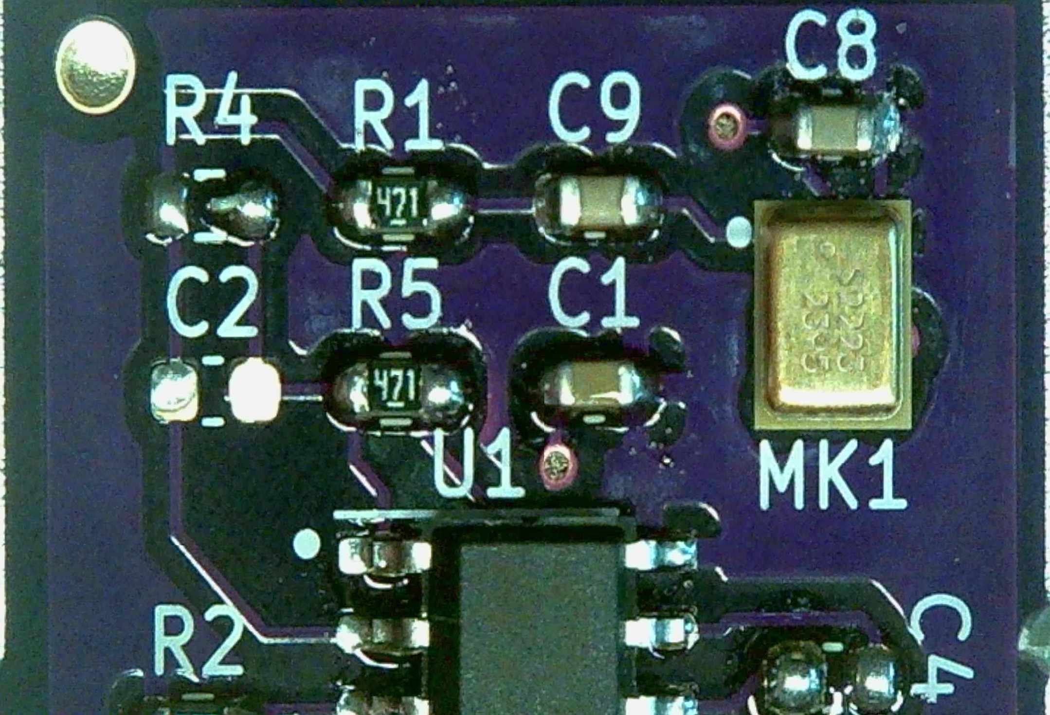

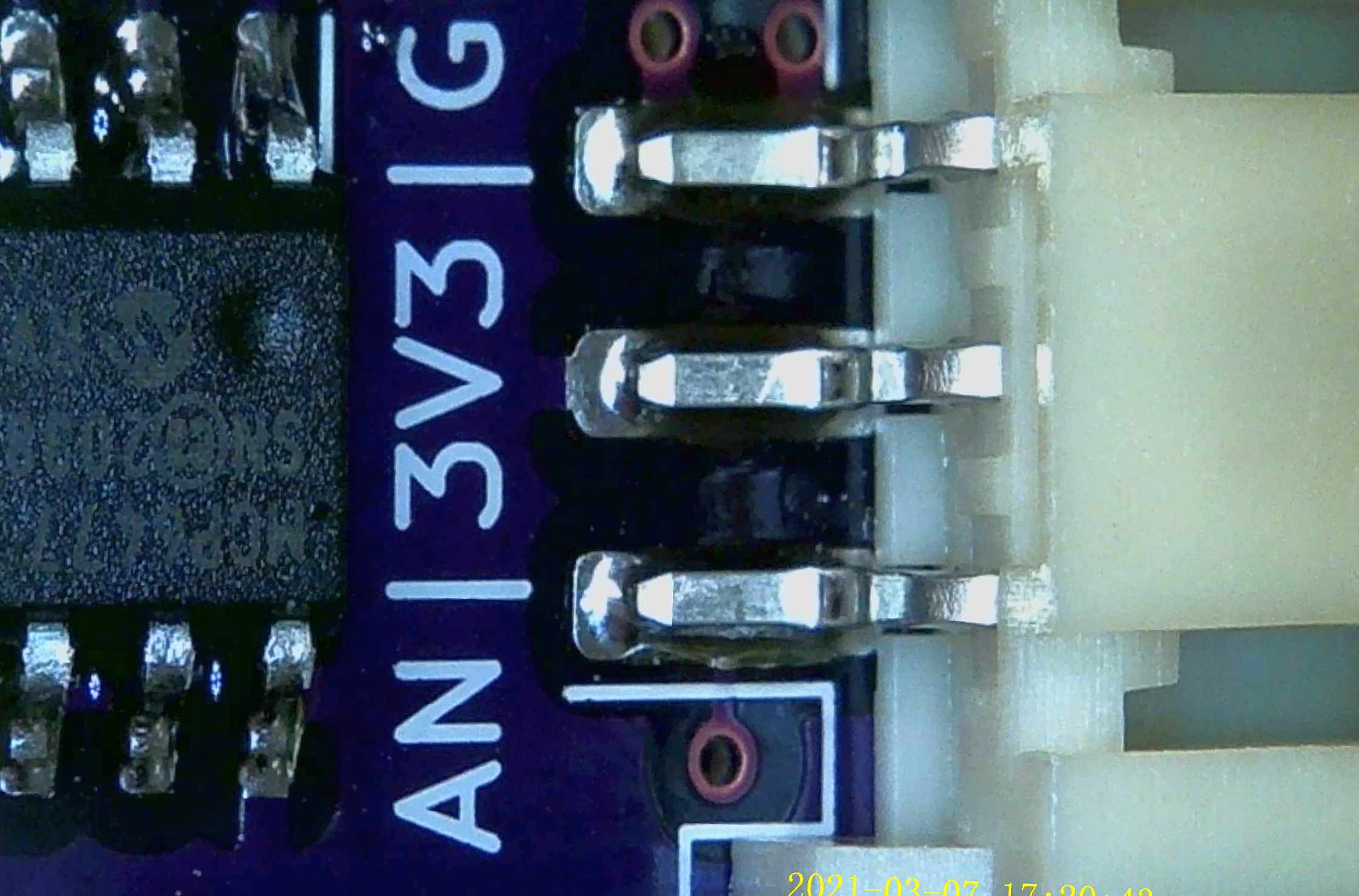
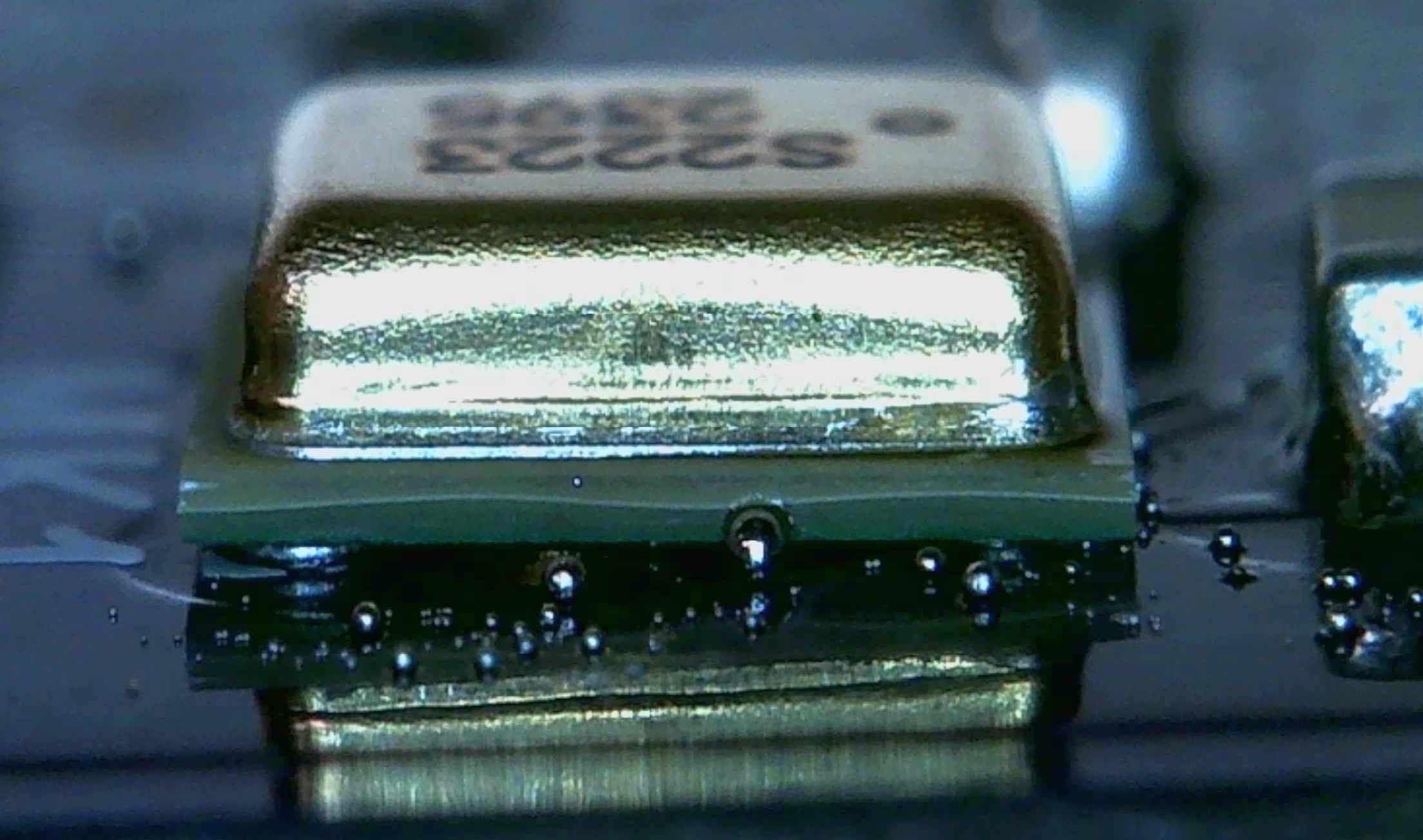
The quality of the images varies a bit depending on lighting conditions. On some of the images after soldering you can also see some 0201 components that are hanging between the pads. I accidentally ordered those 0201 = 0603 metric. Watch out for that. I did not expect those to be soldered properly. For most of them I was able to add some solder manually to bridge the gap. Overall the solder joints on the small 0603 components do not look very "professional", I think mainly due to too much paste applied. Still have to experiment with the nozzles on the syringe there.
The circuit works well so far. I did not have a chance to collect measurements to display them here, but will do that in the future, when probably also some processing of the signals in a connected µC is due. So stay tuned and let me know if you need more details on any of the topics briefly touched upon here.
keep exploring!
cahootOne

